Downlink Project Description
Aaron Wilson
Contents
|
Introduction & Background |
|
Setup of Project |
|
Injection |
|
-analog |
|
-digital |
|
Extraction |
|
-analog |
|
-digital |
|
Observations & Continuations |
Intro
|
The Skeyeball project is an ongoing project in the Indiana University System Design Methods Laboratory for both graduate and undergraduate students to perform embedded system design and implement various projects. The downlink portion of the project involves transfering data from the plane to the ground by using a single signal. My downlink project involves re-implementing Prashant Patel's project from thesummer of 2000, then compacting and debugging it to achieve the desired operation. The first step is to implement the xilinx code using two Logic Engine Boards to host the plane and ground implementation seperately so that adequate testing with the RF transmitter and receiver can be accomplished. I also re-implemented the analog injection and extraction ciruits with new designs to increase bandwidth. A NTSC signal is generated by the video source and it's horizontal and vertical synchronizing pulses allow data to be injected at spaces in the signal where the video signal is retracing to the top of the screen and is always black. The data can be injected in these spots and then extracted from the same spot by the same manner. Once the data is extracted, the video signal is set back to black so that there are no side effects in the video image displayed on the monitor. 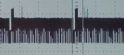 A video frame. 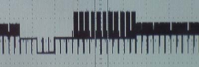 The available 11 spaces with data. 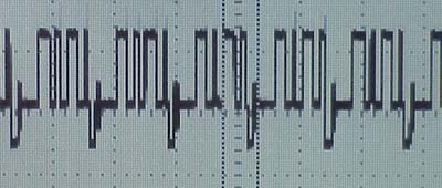 A few spaces with data. 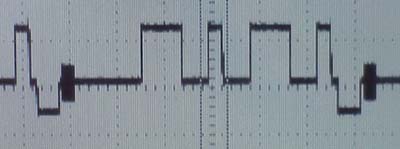 16 bits of data in one space. There are 10 of these spaces in each field and a maximum bandwidth of 300 bits per space. The present goal is an established 56kbps downlink, which is around 90 bits per space. The limitation to higher bps is the bandwidth the RF transmitter, receiver and the analog circuitry allows. Maximum bps is determined experimentally. The data is viewed using hyperterminal, so a lower rate is better. Once further parts of the system are operating we can increase the download capabilities. |
Setup of Project
The physical part of the project has to be done in two phases the testing phase and the finished project. When fin\
ished the injection circuitry will be added into the fusilage of the plane, and the extraction circuitry will be o\
n the ground. This diagram illustrates how the fit in to the bigger picture.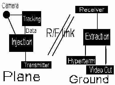 Diagram of Downlink design. For the testing phase I setup the equipment on two Logic Engines. These provided a good foundation to work off of because the have the structure to do wire wrapping and the slots for the neccesary pins. I used the MC1489 and MC1488 chips on the board to send out and recieve the serial communication since they are wired to the serial cables. 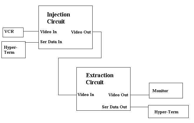 Testing Phase Setup 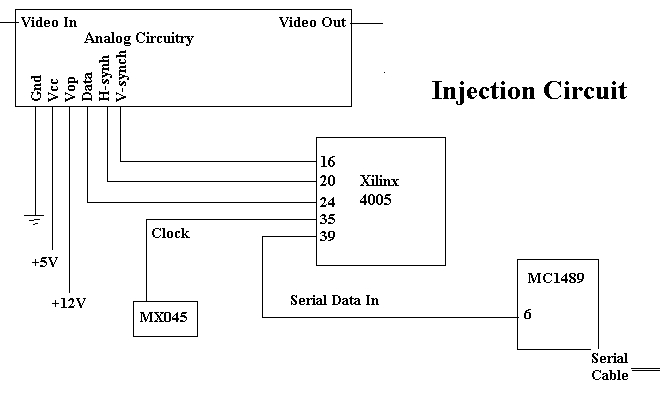 Injection Setup 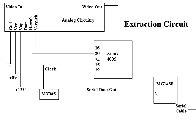 Exctraction Setup 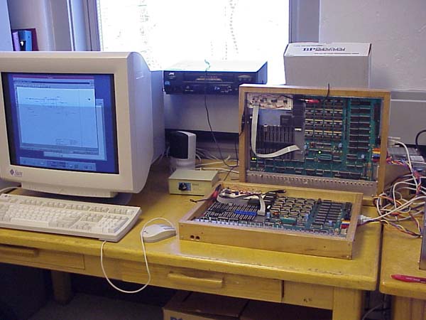 Lab Setup. |
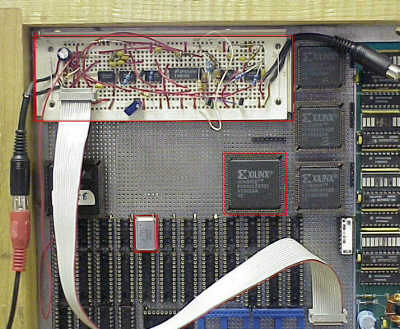
Injection
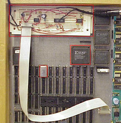
Injection Circuit with breadboard, clock, and xilinx chip highlited.
|
The injection portion of the circuit is divided into two parts, analog and digital. The analog portion was designed by Bryce Himebaugh and implemented on a bread board with individual resistors, capacitors, and transistors, so that refinements could easily be made on it. After a few changes to the resistance and capacitance, the analog portion was behaving as expected. This portion is given the video signal and then using a signal synch separator sends the vertical and horizontal synch pulses to the digital portion, it then receives the data back during the correct pulses in the vertical retrace. Schematic: pdf ps Circuit Description: pdf ps 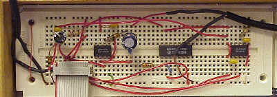
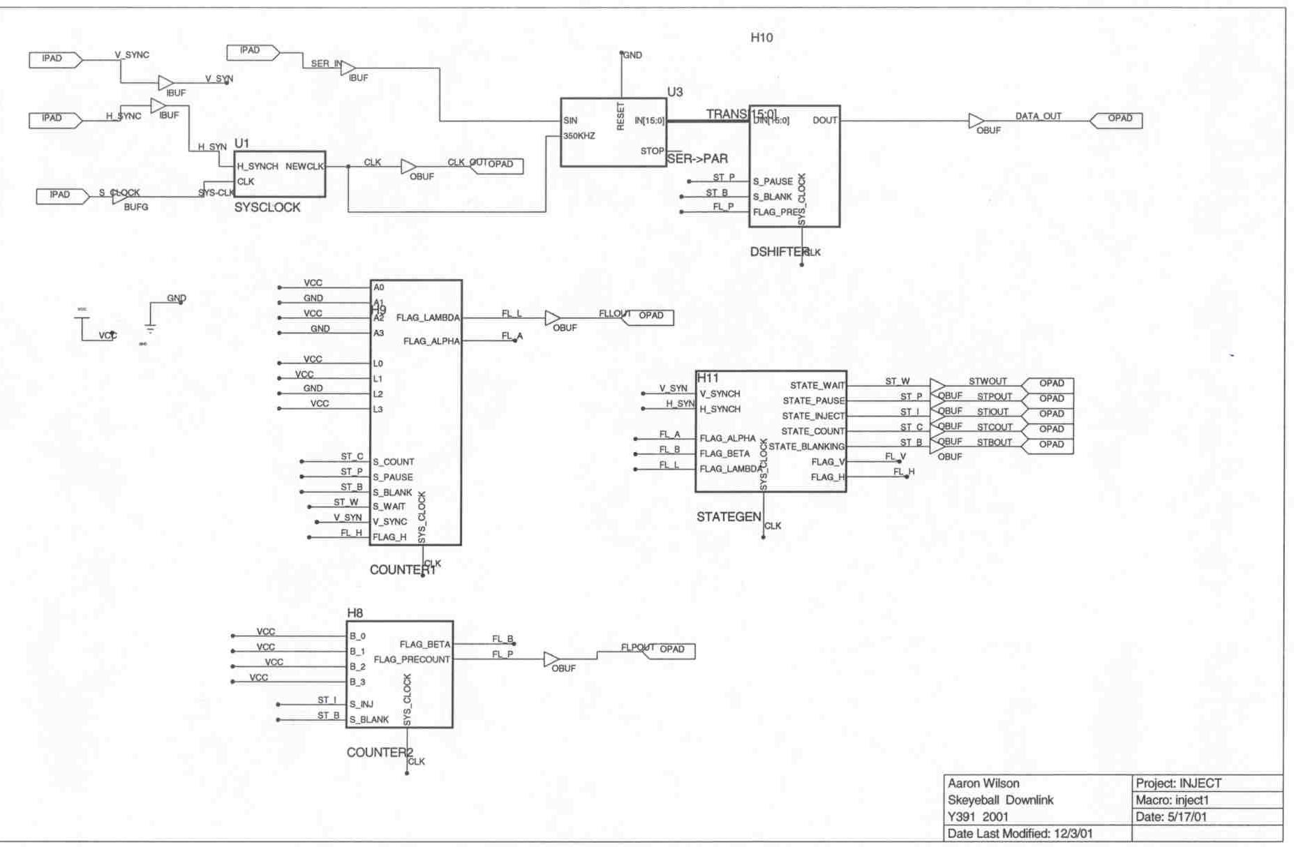
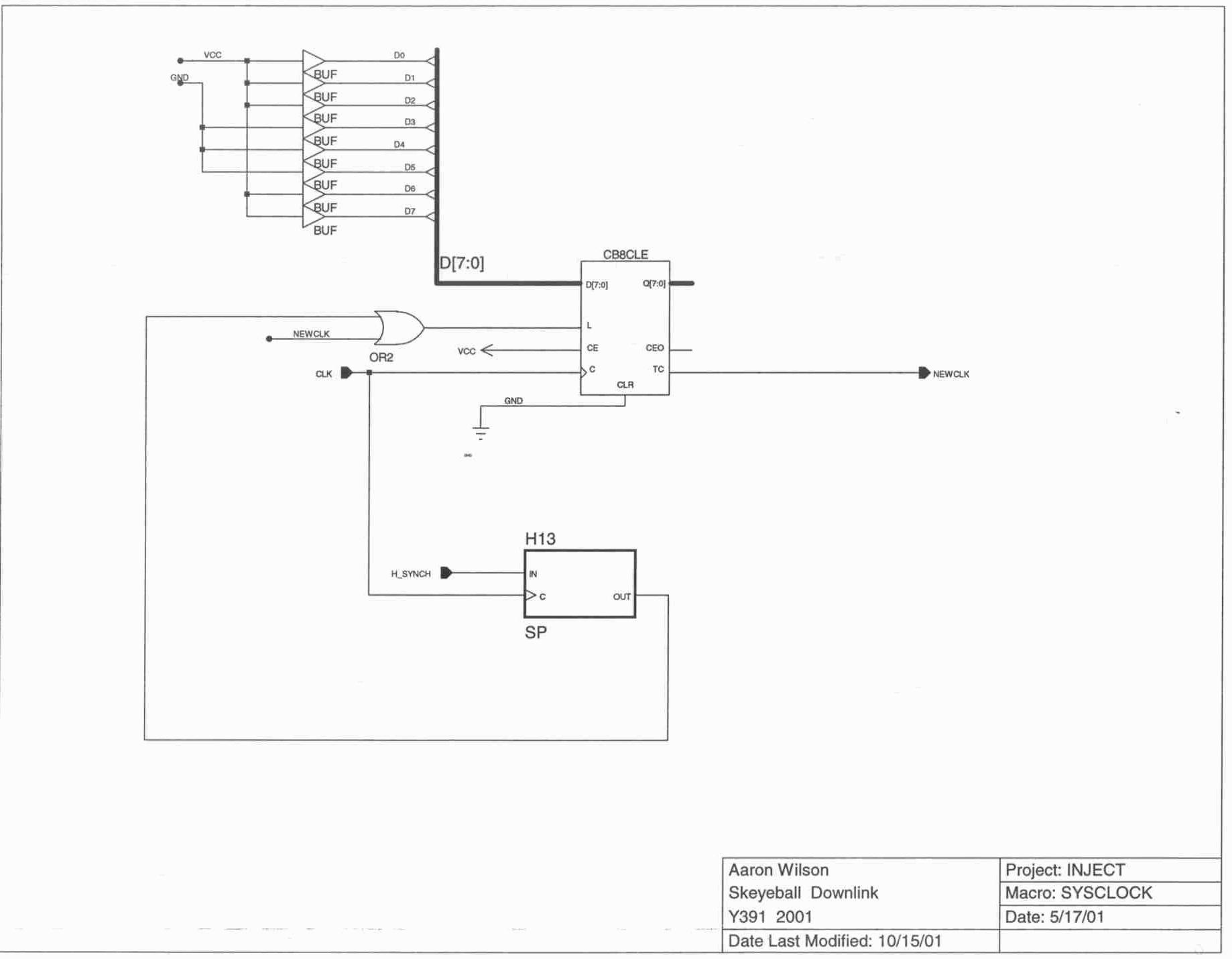
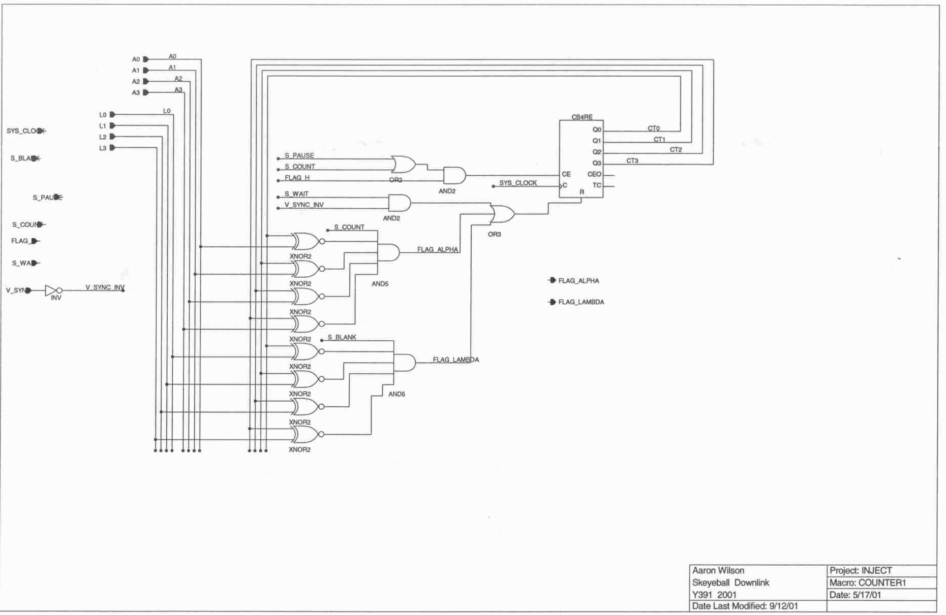
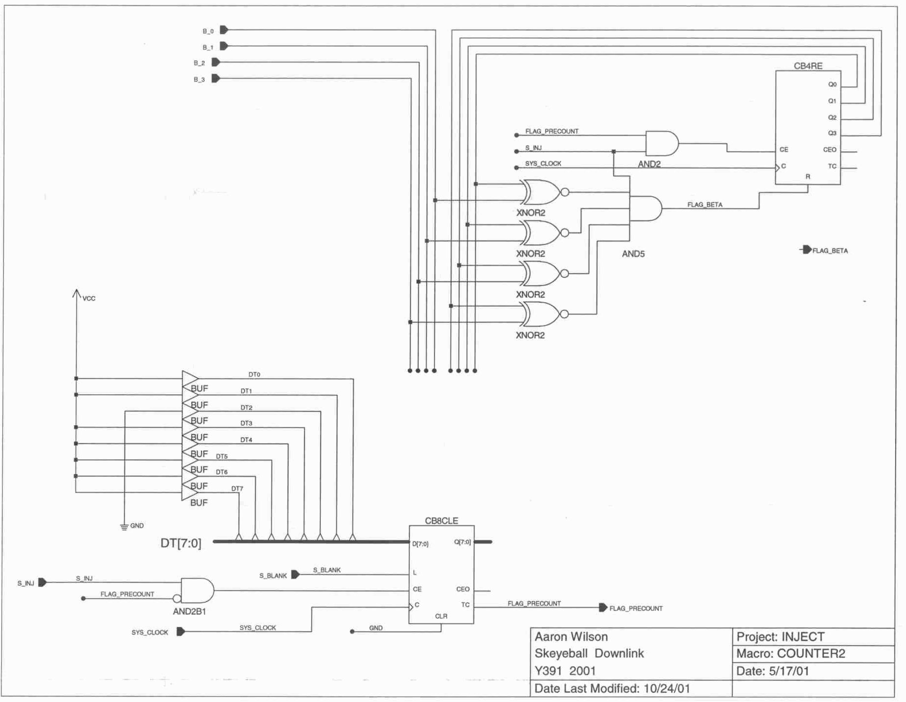
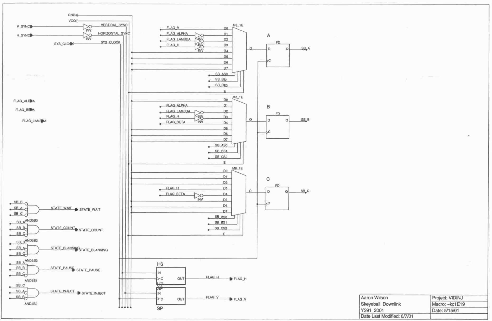
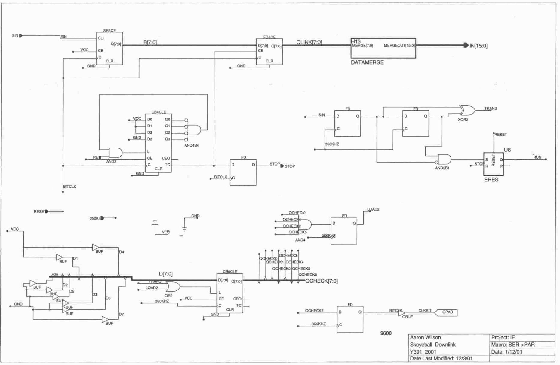
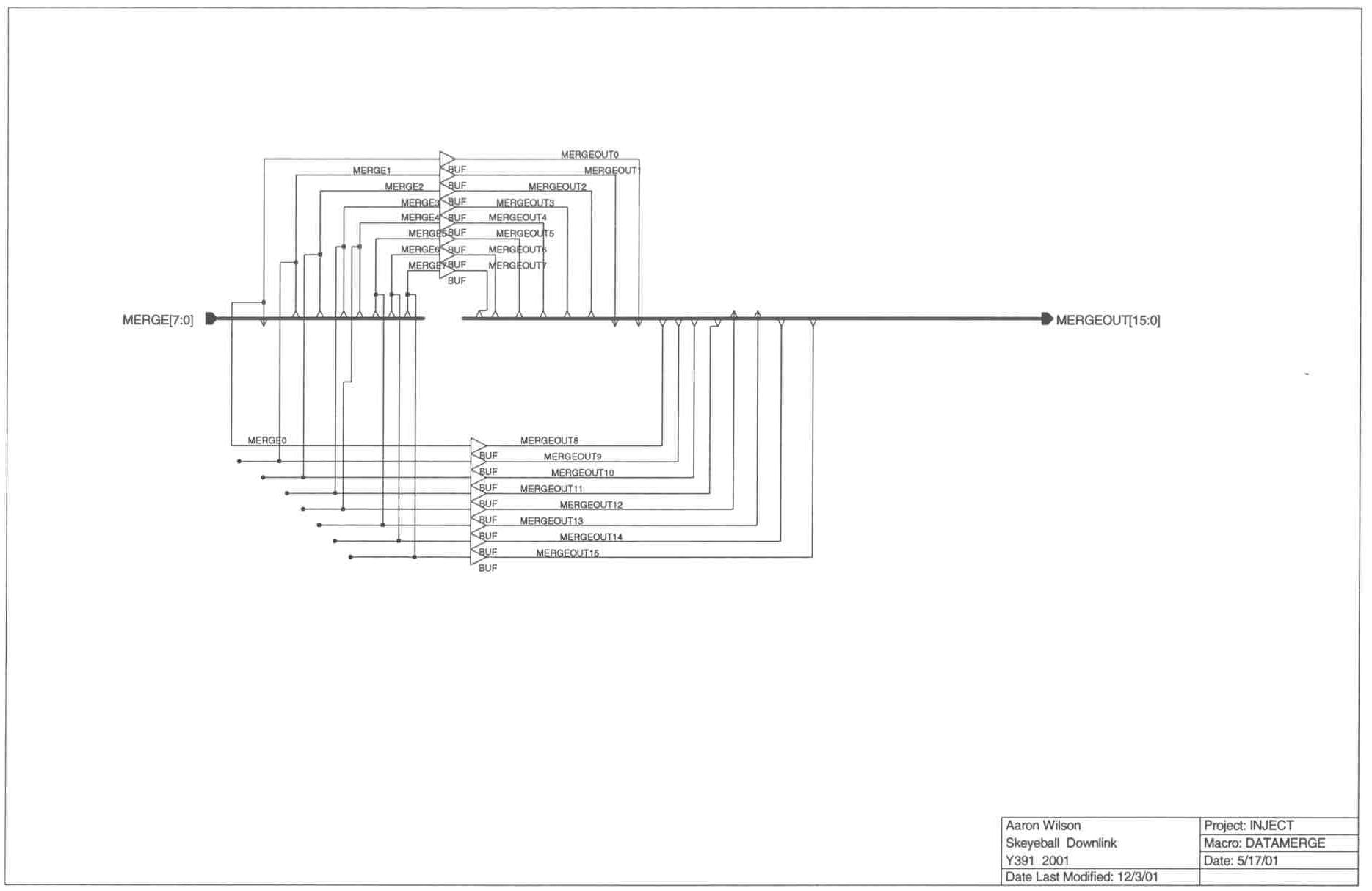
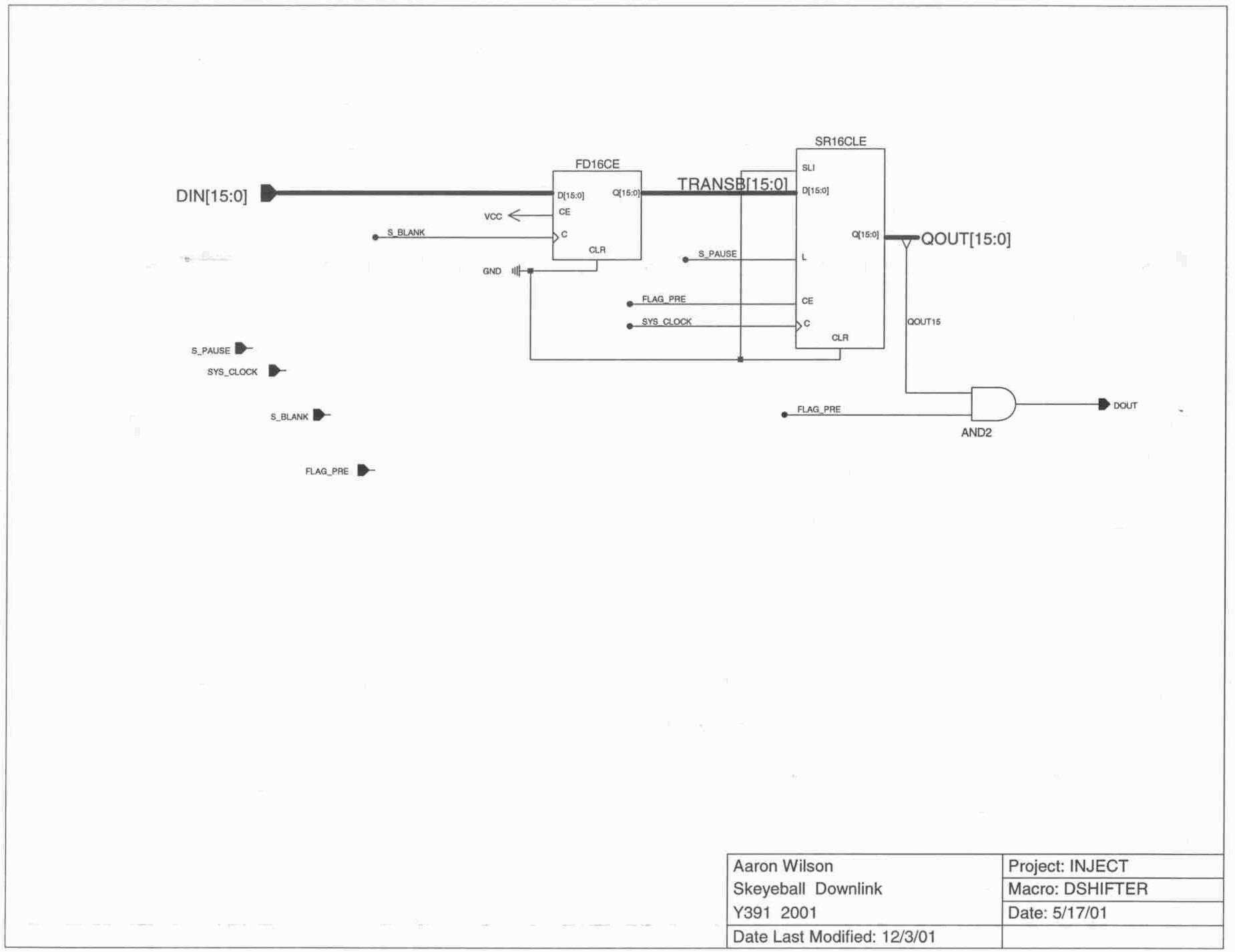
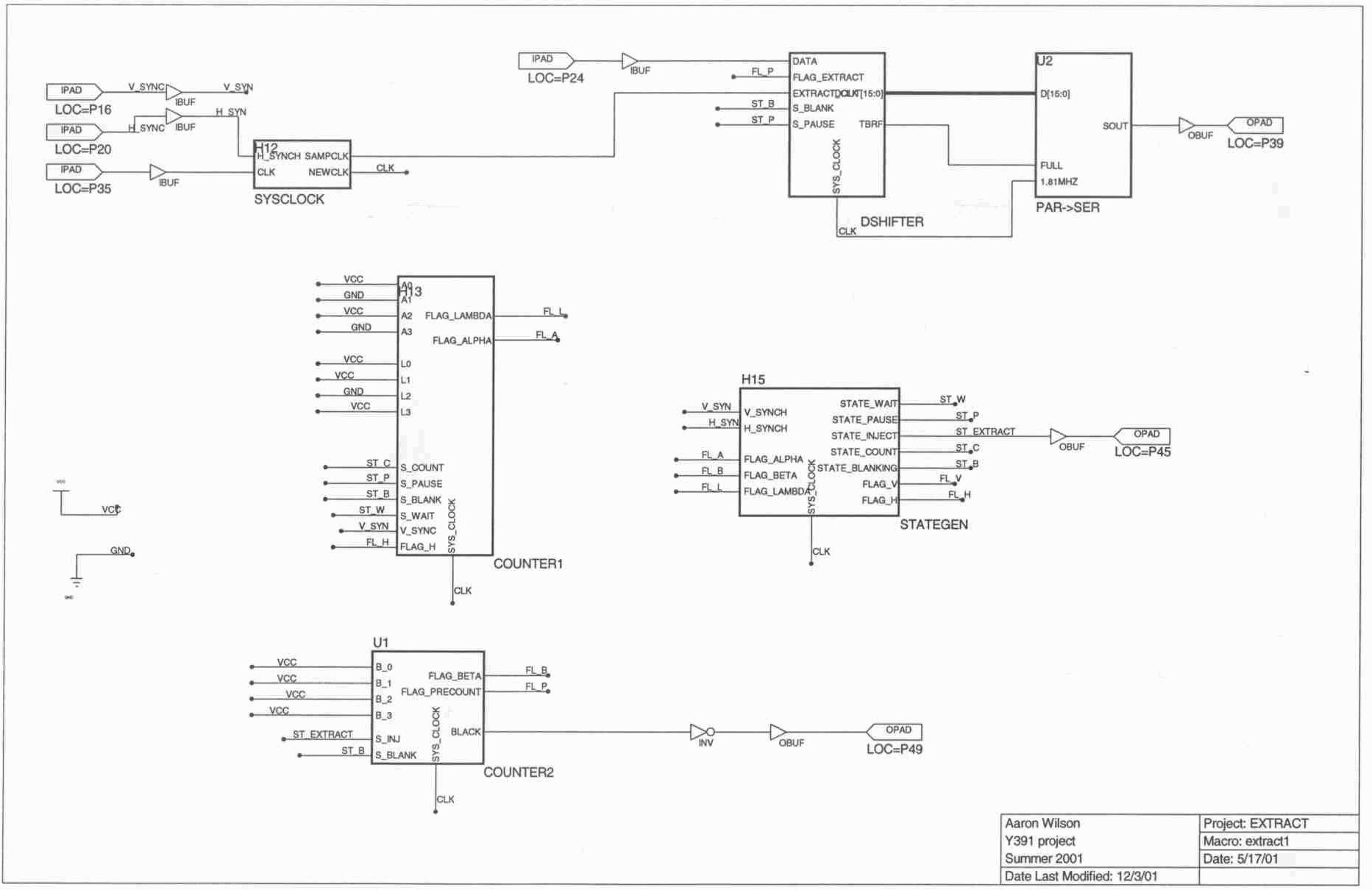
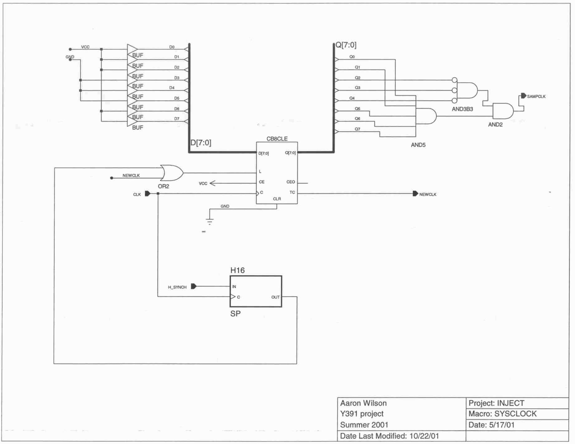
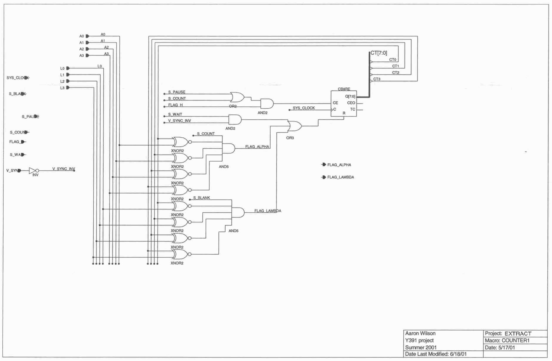
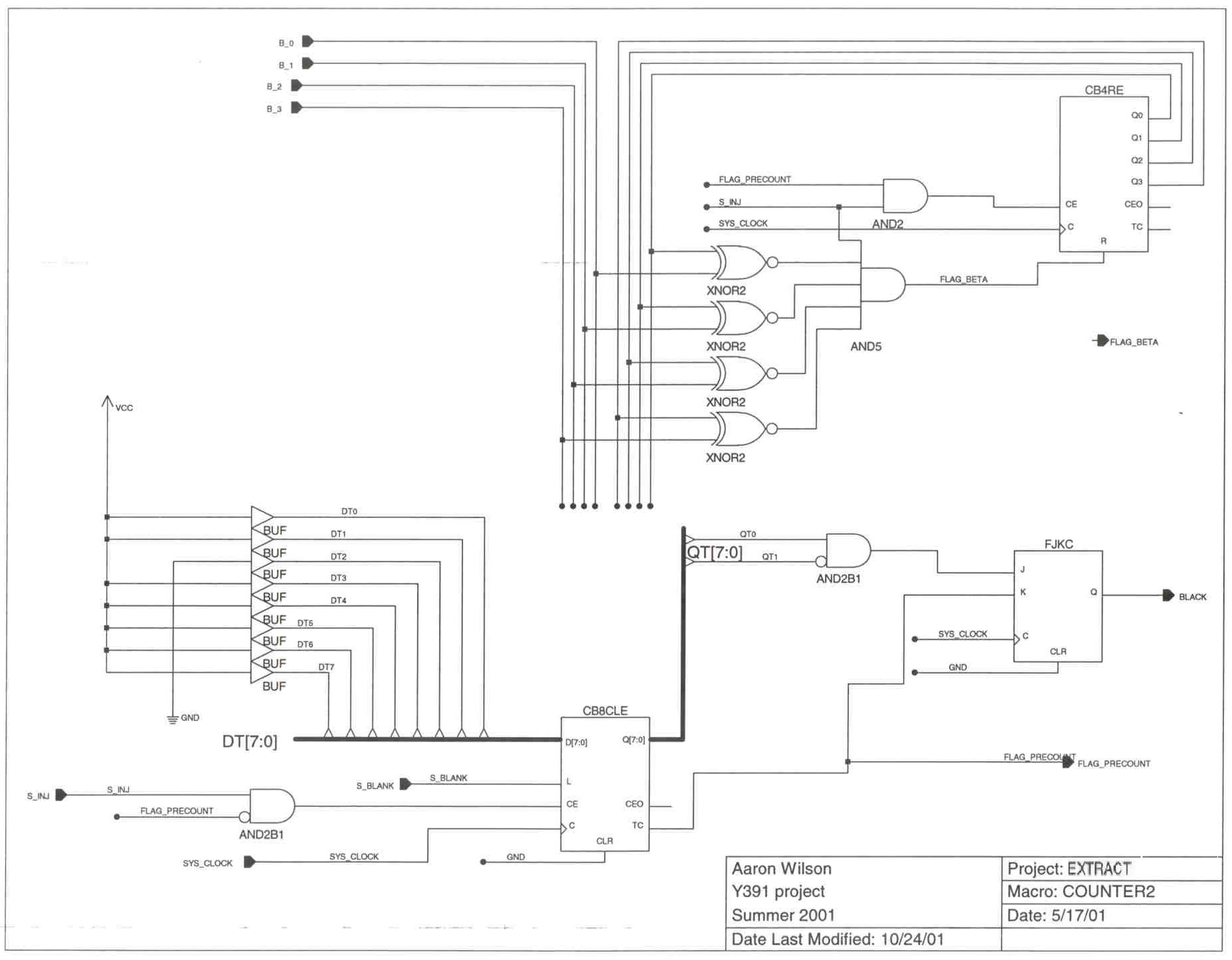
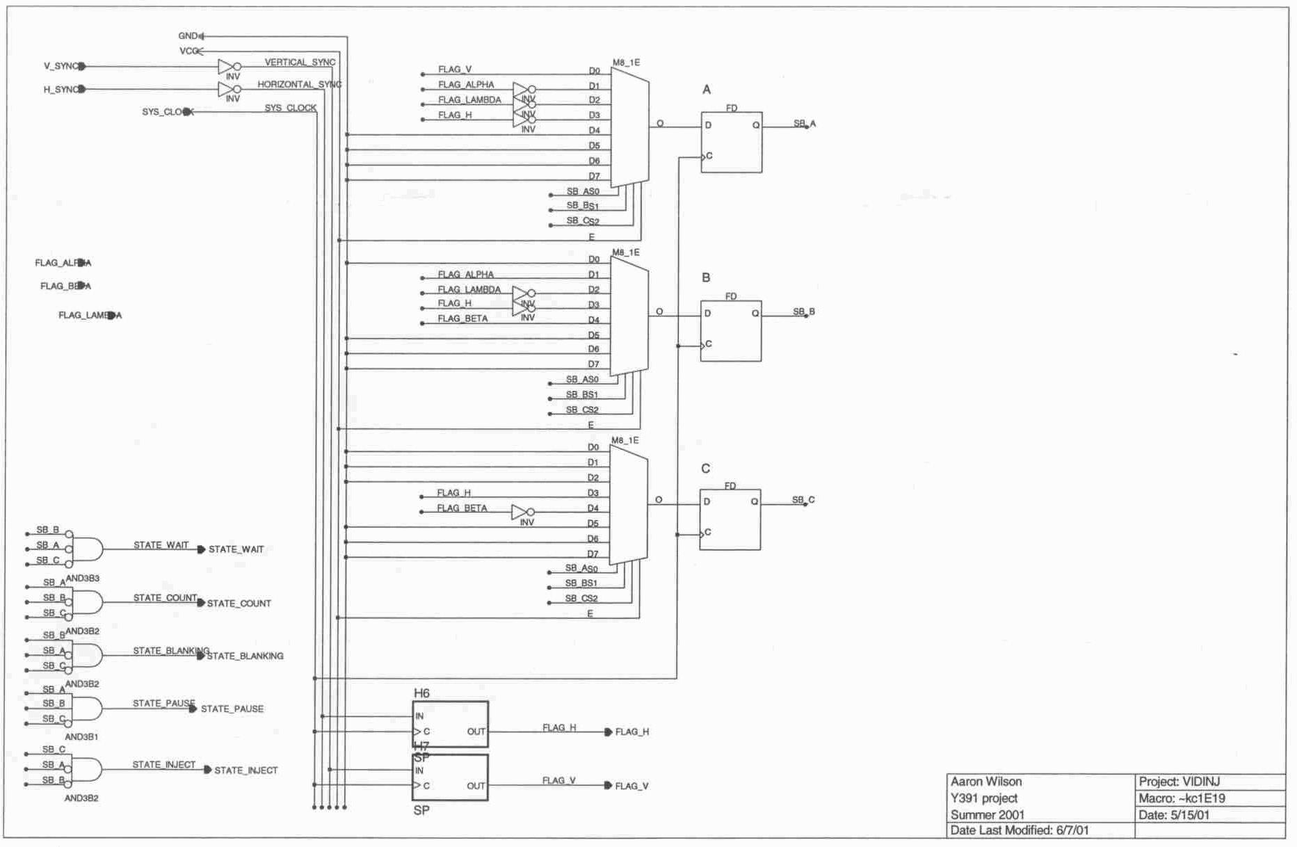
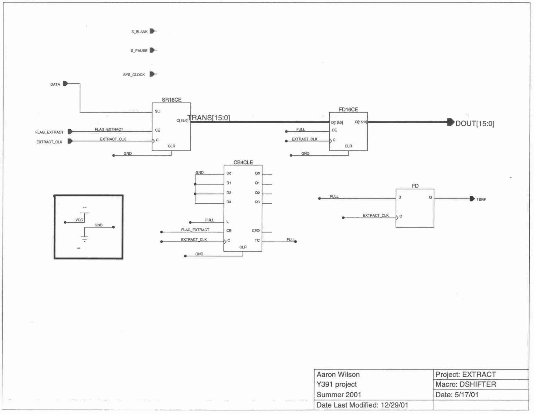
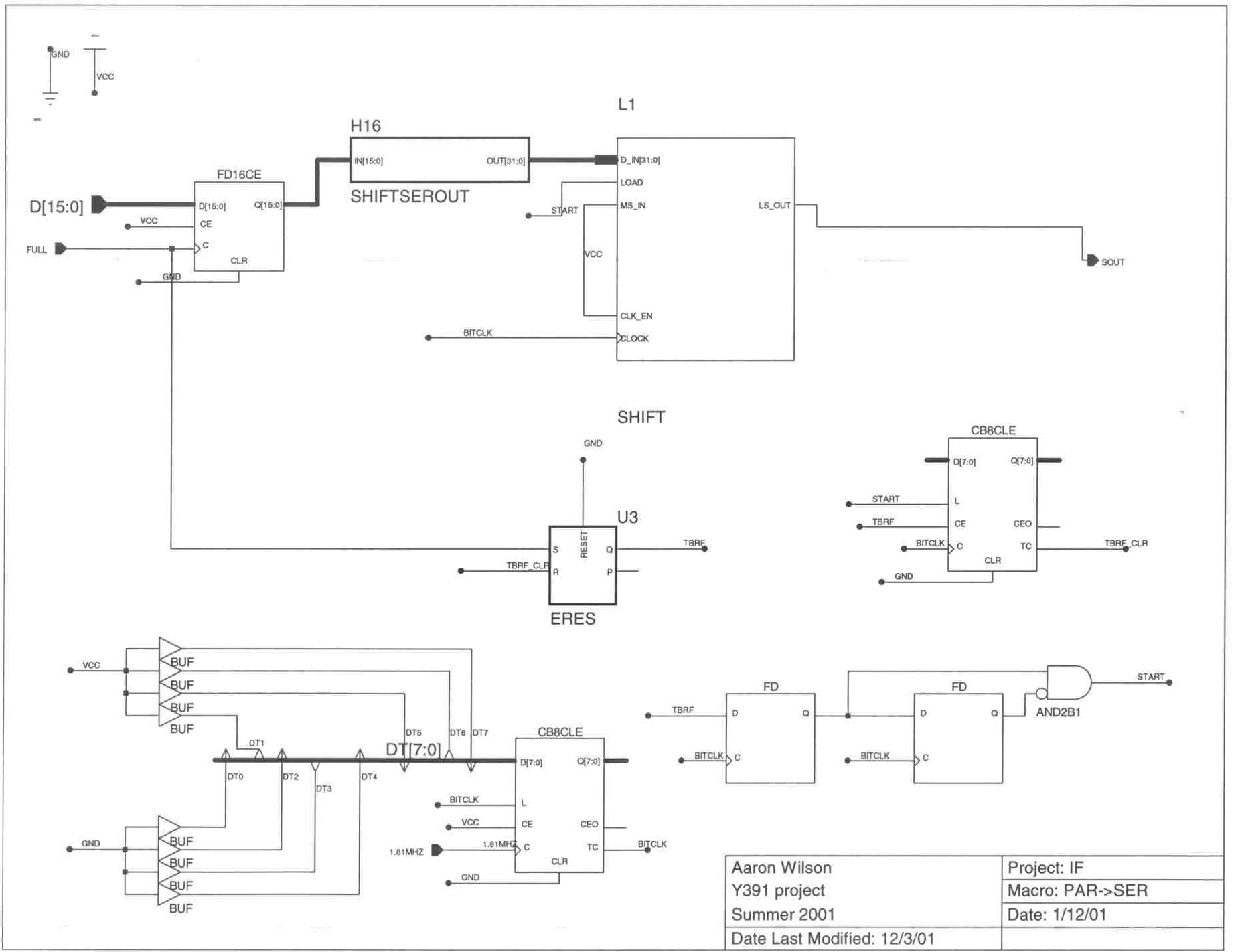
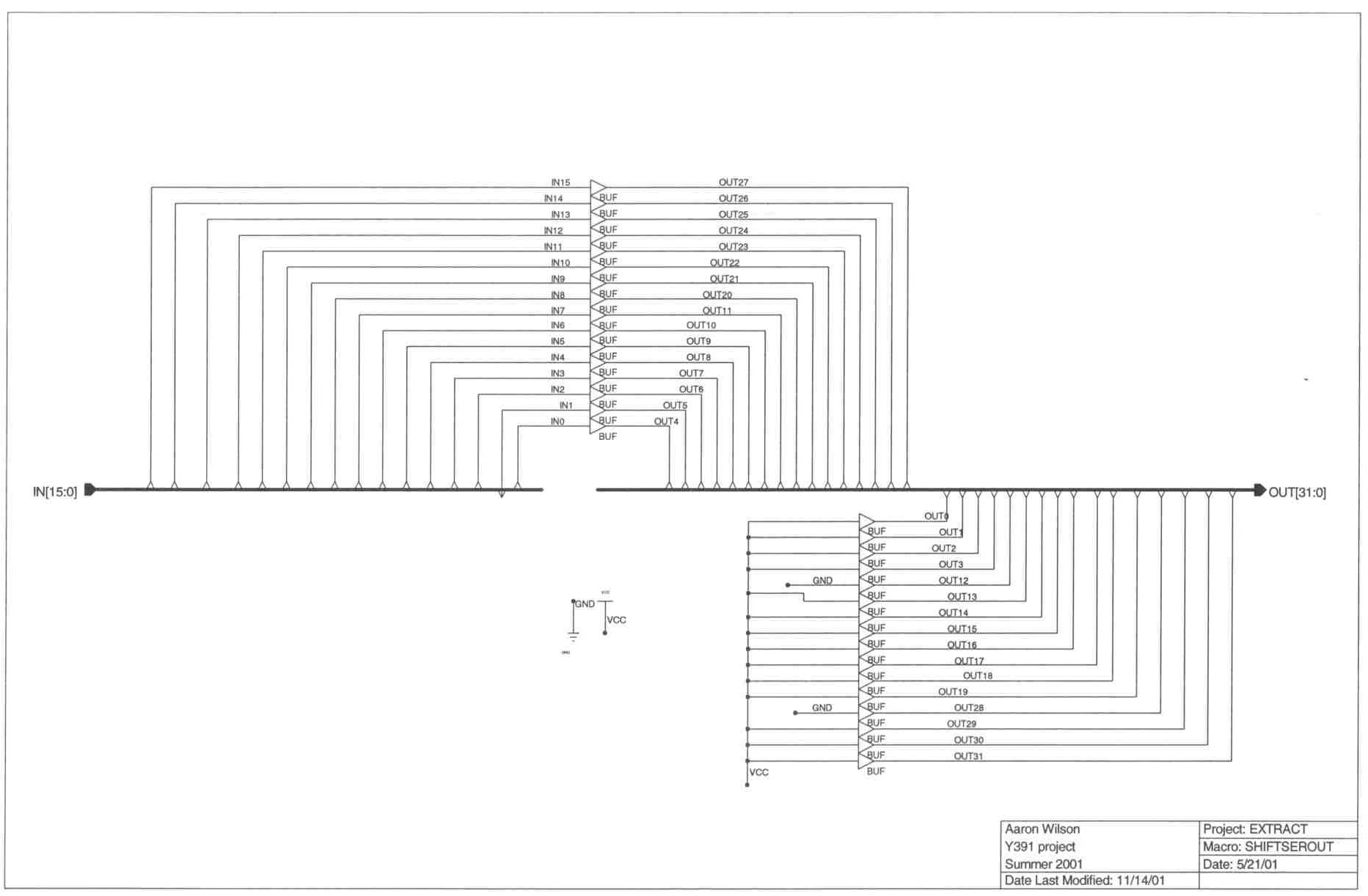
Analog portion of injection circuit. The digital portion is implemented on the Xilinx 4010 chip. This chip allows ample room for the design, as well as plenty of pins for design usage and testing. The clock is provided by the MX045 chip which gives a 20 MHz pulse which is then divided down to produce the desired data pulse rate. The design takes as input the vertical and horizontal synch pulses from the analog portion of the design. It counts these pulses in order to know when to output the data in the correct spaces. I followed closely to the same design from previous project, and I used macros to show a hiearchy in the design, so it can be viewed from a central design page which can then be viewed. The injection circuit ( Schematic: jpg ps ) has 4 inputs(H-synch,V-synch,video w/data, and clock) and 1 output(serial data out). The six main components in the design are: Sysclock ( Schematic: jpg ps ) - generates the clock which drives the injection rate, as well as the Pulse Width Modulater, which samples the incoming data. Counter1 ( Schematic: jpg ps ) - used for tracking the number of horizontal synch pulses and the number of blank spaces. Counter2 ( Schematic: jpg ps ) - used to count the number of bits which are being injected into each space. Stategen ( Schematic: jpg ps ) - generates the states using the horizontal and vertical synch pulses as well as flags generated from the counters. Ser->Par ( Schematic: jpg ps ) - Takes the incoming serial data in RS232 format and puts it on a 16bit bus. Datamerge ( Schematic: jpg ps ) - This Subcomponet, just duplicates the incoming data twice on the line. DShifter ( Schematic: jpg ps ) - Outputs data on a line at a specified data rate at certain stages in the vertical retrace. |
Extraction
Extraction circuit with breadboard, clock, and xilinx chip highlited.
|
The extraction circuit is also in two main parts, the analog and digital portions. The analog extraction circuit was again designed by Bryce Himebau, and is much more complex than the injection analog circuitry. During the extraction there has to be allowances to sample the black level of the video signal as well as cleaning off the video signal once the data has been extracted. This circuit was again constructed on a breadboard for ease of change and functionality. Schematic: pdf ps Circuit Description: pdf ps 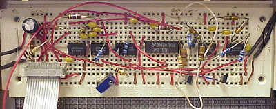
Analog portion of extraction circuit. The digital portion is also implemented on the Xilinx 4005 chip. The clock is again provided by the MX045 chip which gives a 20 MHz pulse which is then divided down to produce the desired data sampling pulse rate. The design takes as input the vertical and horizontal synch pulses from the analog portion of the design. It counts these pulses in order to know when to extract the data from the video signal. As in the injection design I followed closely to the same design from previous project, but used macros to show a hiearchy in the design. The extraction circuit ( Schematic: jpg ps ) has 4 inputs(H-synch,V-synch,serial data in, and clock) and 1 output(data out). The six main components in the design are: Sysclock ( Schematic: jpg ps ) - generates the clock which drives the extraction rate, as well as a clock which is a have clock cycle off of this to use as a sampling clock rate for the data. Counter1 ( Schematic: jpg ps ) - used for tracking the number of horizontal synch pulses and the number of blank spaces. Counter2 ( Schematic: jpg ps ) - used to count the number of bits which are being exracted from each space. Stategen ( Schematic: jpg ps ) - generates the states using the horizontal and vertical synch pulses as well as flags generated from the counters. DShifter ( Schematic: jpg ps ) - Takes the extracted data off the line at the specified data rate and at proper times, and passes it on bus to the Par->Ser component. Par->Ser ( Schematic: jpg ps ) - puts the data on a line in the RS232 standard to be read from computer terminal. ShiftSerialOut ( Schematic: jpg ps ) - Subcomponet to add the appropriate start and stop bits. |
Observations & Continuations
|
The current configuration lets me send serial data from hyperterminal to the injection circuit, and I can observe the data being injected into the line. There are still bugs to be worked out of the downlink design. I have verified that the control signals are being produced at the correct time from the digital design, but there seems to be an irregularity with either the data sampling clock or the data injection clock which is causing them to get out of synch and thus causing irregular data output. Another portion of the injection that also needs to be worked out is the data buffering for the injection portion of the design. In order to inject data into the signal at a high bandwidth, you have to buffer that data, because contrary to the incoming data, the injected data has to be compressed and injected into only the small fraction of the signal which is the vertical retrace. This data buffering could be implemented with a system of counters and ram modules within the Xilinx design. The extraction circuit was observed when the inject rate was slower, but not at the higher rate, it has not been tested since there are still bugs with the injection circuit. |
Aaron Wilson
Skeyeball Downlink
Professor Steven Johnson
rev. by Aaron Wilson