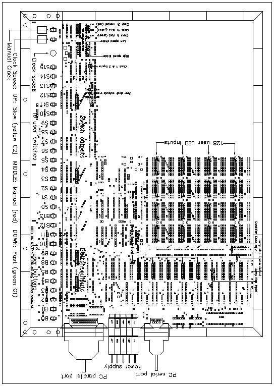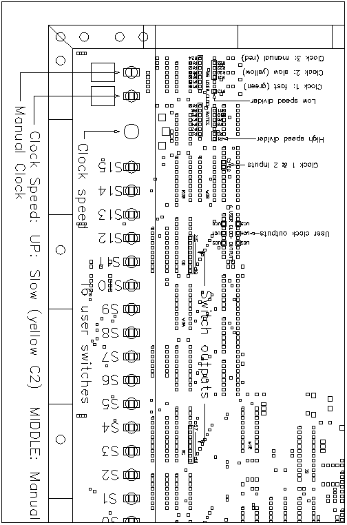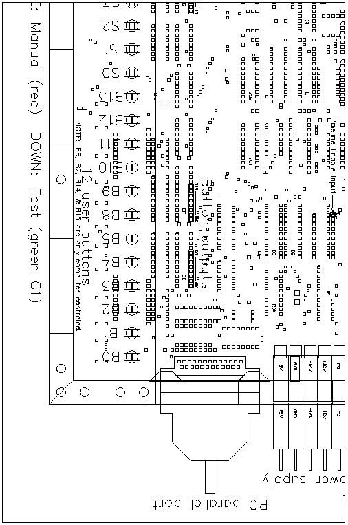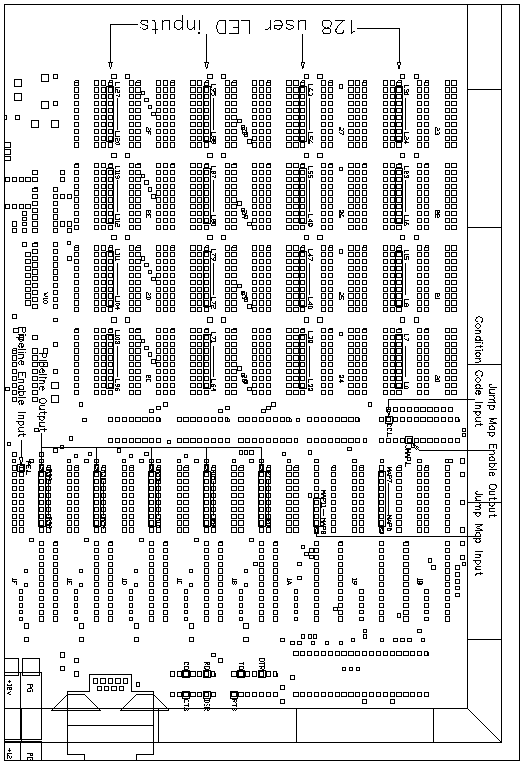
Figure 26 illustrates the Logic Engine board with all the user tie points highlighted and labeled. Figure 27 , Figure 28 , and Figure 29 are detailed drawings of the board. The tie points are wire-wrap pins that can be used by simply wiring from the user design in the prototype area to the tie point. Table 1 below, lists and describes all the tie points on the board.
| Function | Tie Points | Input Output | Illustrated in Figure | Description |
|---|---|---|---|---|
| Clock | D0-D23 | Output | Fig. 27 | Clock Divisor: |
| C1-C2 | Input | Fig. 27 | Clock Selector: | |
| U0-U5 | Output | Fig. 27 | User Clock: | |
| Switches | S0-S15 | Output | Fig. 27 | Switch Outputs: |
| Buttons | B0-B15 | Output | Fig. 28 | Button Outputs: |
| LED's | L0-L127 | Input | Fig. 29 | LED Inputs: |
| Microsequencer | P0-P39 | Output | Fig. 29 | Pipeline Outputs: |
| PE.L | Input | Fig. 29 | Pipeline Enable: | |
| MAP0-MAP11 | Input | Fig. 29 | Jump Map Inputs: | |
| JMAP.L | Output | Fig. 29 | Jump Map Enable: | |
| CC.L | Input | Fig. 29 | Condition Code: | |
| Serial Port | DTR | Input | Fig. 29 | |
| TD | Input | Fig. 29 | ||
| RTS | Input | Fig. 29 | ||
| RD | Output | Fig. 29 | ||
| CD | Output | Fig. 29 | ||
| DSR | Output | Fig. 29 | ||
| CTS | Output | Fig. 29 |
The clock supplied on the board is a variable rate
clock with three selectable modes of operation. Each mode can
be selected using the three position toggle switch located in
the lower left corner of the board. The three positions are down:
fast clock rate, up: slow clock rate, and middle: manual clock.
The modes are also indicated by the lights above the switch:
green: fast clock rate, yellow: slow clock rate and red: manual
clock. The exact range of rates of the fast and slow mode can
be selected by wiring from tie points C1 (fast) and C2 (slow)
to one of the clock divisor tie points. This should already be
set to some default configuration. In these two modes, the frequency
can be adjusted with the clock pot. To increase the frequency,
turn the pot clockwise, to decrease, turn it counter clockwise.
When the clock is in manual mode, it is controlled by the push
button in the lower left corner of the board. When the button
is depressed, the clock is high, when released, the clock is low.
There are six tie points (U0 - U5) on the board for
access to the user clock. They are all generated from the same
signal run through separate buffers.
There are 16 switch tie points (S0 - S15) and 16
button tie points (B0 - B15) on the Logic Engine board. All of
the switches and 12 of the buttons can be controlled in manual
mode from the switches and buttons across the front of the board.
The 16 switches on the board starting on the right, are connected
to tie points S0 - S15. The 12 buttons on the board starting
on the right, are connected to tie points B0 - B5 and B8 - B13.
In manual mode, when a switch is positioned toward the front
of the board, the value on the correspoding tie point is low (0V).
When positioned away from the front of the board, the value is
high (5V). In manual mode, when a button is in the up position,
the value on the correspoding tie point is low (0V). When in
the down position, the value is high (5V).
When in host mode, all 32 of the switch and button
tie points can be controlled from the host computer. In this
case the switches and buttons on the board are disconnected from
the tie points and have no effect on these signals. Refer to
the proper chapter for information on how each software tool can
control the switches and buttons.
There are 128 LED's that can be used to display signals.
They are used by wire wrapping the signal to be displayed to
one of the LED tie points (L0 - L128). The values of the LED's
and hence the value of any signal wired to an LED can be read
by software when in host mode. Refer to the proper chapter for
information on how each software tool can control the switches
and buttons.
The prototype area has a power grid on each side.
The top side has a grid of 5V. And the bottom side has a grid
of 0V. To place a socket in the prototype area, insert the socket,
and make a solder bridge from the Vcc pin to the grid on the top
side and make a solder bridge from the GND pin to the grid on
the bottom side. Alternatively, you can use stake pins. Solder
these to the top and bottom grids and wire wrap from these to
the socket.
[Contents]
[0 Logic Engine Programmer Interface]
[Logic Engine User's Manual]

Figure 27. The Lower Left Corner of the Logic Engine Board

Figure 28. The Lower Right Corner of the Logic Engine Board

Figure 29. The Upper Right Corner of the Logic Engine Board